MesoGlue Replacing Hot Solder Could Improve Every Device With Circuit Boards

A team led by Prof. Hanchen Huang of Northeastern University has discovered a new way to merge metals at room temperature, without heat by developing a new material called ‘MesoGlue’. Soldering techniques have improved a lot and in large scale circuit board production, most parts of it have been automated. But one thing has remained unchanged throughout the evolution of circuit boards; the hot solder. There has never been another way to attach electronic components to a PCB without melting iron. Not until now.

mesoglue-heatsink-demo.

MesoGlue is a combination of metal and glue. The creators have used metallic nanorods with cores coated with elements Indium and Galium on either side of the two surfaces that need to be joined. When the two surfaces come in contact, the nanorods are interlocked, and form a liquid which is solidified by the core of the rods. The resulting bond acts like both, a conductor and a glue. The technology has been patented through Northeastern University.

The bond formed by the MesoGlue is matchless as it provides thermal and electrical conductivity like metal bonds, resistant to high temperature and air leaks. The applications are as wide as attaching miniature components to circuit boards, and attaching metal pipes without welding.

mesoglue-metallic-glue-replaces-solder.

Small circuit components like processors, capacitors and resistors tend to lose their intended potential when heated to attach them to the circuit board. That is why soldering should be done very quickly, and with the smallest drop of iron as possible. This MesoGlue allows fusion of metals without having to heat them.

Though in its early stages, a company founded by Prof. Hanchen, Paul Elliot and Prof. Stephen Stagon has begun mass-producing this glue for commercial applications. By eliminating the need for heat, this metallic glue could improve the performance of every device that has circuit boards in them.

Researchers developing new thermal interface materials

In the microelectronics world, the military and private sectors alike need solutions to technological challenges. Dr. Mustafa Akbulut, assistant professor of chemical engineering, and two students lead a project funded by DARPA to create thermal interface materials (TIMs) that have a superior ability to transfer heat and a strong capacity to keep cool.

In evaluating a central processing unit, as an example, there are many pieces that individually need temperature management. “As you get smaller and smaller, there is higher heat dissipation per unit area. Locally, you have higher temperatures…you have a harder time operationally—you need better thermal interface materials. This is especially important for radars, laser systems and also for military electronics,” said Akbulut.
Essentially and most critically, the device needs the ability to avoid overheating. As Akbulut asserts, “unless you cool it, it fails.”
In evaluating an electronic device and a cooling system that need to be placed together as they function, if there is an absence of thermal material in between, the heat created by the electronic device can potentially erode the device. According to Akbulut, non-soft materials are considered less effective as a TIM because they do not adequately cover all interior openings or gaps, even though the naked eye may not detect this space.
Akbulut explains why optimal contact is not achieved through current technology. “If you look at the very fine scale, [these two pieces] are not smooth. If you look at these with an electron microscope, you see they are like mountains. If you bring these surfaces together, they do not have perfect contact.” Thus, the objective of a traditional TIM is not fully met.
Soft materials, including paste, often minimize the gap, said Akbulut. The invention of his new metal-based, soft material leads to high thermal conductive activity and because of its malleable nature, consistent contact is achieved. His research group has recently developed TIMs with thermal conductivity greater than 100 W/m-k and elastic modulus values in the order of 20 GPa, significantly advancing the current state of art for TIMs. As a comparison, this material is ten times softer than steel and three times more thermally conductive.
Using copper and nano-materials together, Akbulut believes his new TIM can lead to greater optimization and large-scale implementation in the future.

Nusselt Number

In heat transfer at a boundary (surface) within a fluid, the Nusselt number (Nu) is the ratio of convective to conductive heat transfer across (normal to) the boundary. In this context, convection includes both advection and diffusion. Named after Wilhelm Nusselt, it is a dimensionless number. The conductive component is measured under the same conditions as the heat convection but with a (hypothetically) stagnant (or motionless) fluid. A similar non-dimensional parameter is Biot Number, with the difference that the thermal conductivity is of the solid body and not the fluid.

A Nusselt number close to one, namely convection and conduction of similar magnitude, is characteristic of “slug flow” or laminar flow. A larger Nusselt number corresponds to more active convection, with turbulent flow typically in the 100–1000 range.

The convection and conduction heat flows are parallel to each other and to the surface normal of the boundary surface, and are all perpendicular to the mean fluid flow in the simple case.


where h is the convective heat transfer coefficient of the flow, L is the characteristic length, k is the thermal conductivity of the fluid.

Selection of the characteristic length should be in the direction of growth (or thickness) of the boundary layer; some examples of characteristic length are: the outer diameter of a cylinder in (external) cross flow (perpendicular to the cylinder axis), the length of a vertical plate undergoing natural convection, or the diameter of a sphere. For complex shapes, the length may be defined as the volume of the fluid body divided by the surface area.
The thermal conductivity of the fluid is typically (but not always) evaluated at the film temperature, which for engineering purposes may be calculated as the mean-average of the bulk fluid temperature and wall surface temperature.
In contrast to the definition given above, known as average Nusselt number, local Nusselt number is defined by taking the length to be the distance from the surface boundary to the local point of interest.


The mean, or average, number is obtained by integrating the expression over the range of interest, such as:[2]


The mass transfer analog of the Nusselt number is the Sherwood number.

New Method for Enhancing Thermal Conductivity Could Cool Computer Chips

The surprising discovery of a new way to tune and enhance thermal conductivity gives engineers a new tool for managing thermal effects in smart phones and computers, lasers and a number of other powered devices.

The finding was made by a group of engineers headed by Deyu Li, associate professor of mechanical engineering at Vanderbilt University.

Li and his collaborators discovered that the thermal conductivity of a pair of thin strips of material called boron nanoribbons can be enhanced by up to 45 percent depending on the process that they used to stick the two ribbons together. Although the research was conducted with boron nanoribbons, the results are generally applicable to other thin film materials.

One of the remarkable aspects of the effect Li discovered is that it is reversible. For example, when the researchers wetted the interface of a pair of nanoribbons with isopropyl alcohol, pressed them together and let them dry, the thermal conductivity was the same as that of a single nanoribbon. However, when they wetted them with pure alcohol and let them dry, the thermal conductivity was enhanced. Then, when they wetted them with isopropyl alcohol again, the thermal conductivity dropped back to the original low value.

One of the first areas where this new knowledge is likely to be applied is in thermal management of microelectronic devices like computer chips. Today, billions to trillions of transistors are jammed into chips the size of a fingernail. These chips generate so much heat that one of the major factors in their design is to prevent overheating. In fact, heat management is one of the major reasons behind today’s multi-core processor designs.

Thermal invisibility cloak improves electronics heat distribution

A thermal invisibility cloak that can make objects thermally invisible by redirecting incoming heat has been developed by Singaporean researchers.
Based on carefully engineered metamaterials – materials with properties that can’t be found in nature – the technology could potentially help improve the thermal performance of various electronic systems by fine-tuning thermal dissipation.
The team from the Nanyang Technological University (NTU) that developed the system has previously experimented with the so-called passive thermal cloaks capable of guiding conductive heat around a hidden object.
The team’s latest invention is the first active thermal invisibility cloak with an on/off switch and the ability to be adapted to objects of varying geometries.
“We considered the question of whether we can control thermal cloaking electrically, not by guiding heat around the hidden object passively with traditional metamaterials, but by ‘pumping’ heat from one side of the hidden object to the other side actively, with thermoelectric modules,” said Professor Baile Zhang, the lead researcher behind the project. The work is described in an article featured on the cover of the latest issue of the journal Applied Physics Letters.
Zhang said the device could help optimise the thermal performance of a large variety of electronic devices including high-power engines, magnetic resonance imaging instruments and thermal sensors.
The active thermal cloak consists of 24 small thermoelectric semiconductor heat pumps controlled by an external input voltage. These heat-pumps are distributed around a 62-millimeter diameter air hole in a carbon steel plate just 5mm thick.
When electrical current runs through the junction between two modules, the so-called Peltier effect kicks in and removes or generates heat.

New Material to Decrease Energy Usage in Electronics

Researchers have determined that gallium nitride (GaN) could become the next best semiconductor for electronics because it would immensely cut energy usage.

Cambridge Electronics Inc. (CEI) has announced a new line of GaN transistors and power electronic circuits. This line promises to reduce energy usage by 10 to 20 percent in consumer electronics, data centers and electric cars by 2025. CEI plans to use these transistors to make data centers use less energy, electric cars more powerful and cheaper to build and power adapters one-third of the size, according to Phys.org.

“CEI’s GaN transistors have at least one-tenth the resistance of such silicon-based transistors, according to the company. This allows for much higher energy-efficiency, and orders-of-magnitude faster switching frequency—meaning power-electronics systems with these components can be made much smaller,” according to Phys.org.

Typically GaN transistors have not been in the market because of safety issues and high manufacturing costs. “Power transistors are designed to flow high currents when on, and to block high voltages when off. Should the circuit break or fail, the transistors must default to the ‘off’ position to cut the current to avoid short circuits and other issues—an important feature of silicon power transistors. But GaN transistors are typically ‘normally on’—meaning, by default, they’ll always allow a flow of current, which has historically been difficult to correct,” according to Phys.org.

Researchers have addressed these issues by modifying the GaN transistor structure and developing transistors that are ‘normally off.’

“To make traditional GaN transistors, scientists grow a thin layer of GaN on top of a substrate. The MIT researchers layered different materials with disparate compositions in their GaN transistors. Finding the precise mix allowed a new kind of GaN transistors that go to the off position by default,” according to researchers.

New Technology Improves Heat Dissipation Performance

OKI Circuit Technology in Japan has developed a mass-production technology for multi-layer copper-coin printed circuit boards that supports high speeds and high frequencies.

The technology is a T-Coin (Technology of copper coin insert) structure that has the shape and thickness of copper coins; it improves heat dissipation, prevents damage, and increases reliability and thermal conductivity. The technology is available in a wide range of copper coin diameters from 3.0 mm to 6.0 mm and printed circuit board thicknesses from 1.0 mm to 2.0 mm.

“Materials designed for use at high speeds and high frequencies tend to have lower structural strength than conventional printed circuit boards. Inserting copper coins, which subjects through-holes to loads, was previously considered difficult for multi-layer boards. The conventional mainstream method for ensuring heat dissipation has been “through-hole construction,” whereby many through-holes are drilled in the printed circuit board and their surfaces are copper-plated to dissipate heat. However, with electronic components packed at ever-greater densities to handle ever-higher data volumes, the amount of heat to be dissipated has increased, while the space available for providing through-holes to dissipate heat has shrunk. This trend has made measures for achieving adequate heat dissipation an increasingly urgent issue,” according to Business Wire.

“The T-Coin increases the area available for heat conduction for a limited number of through-holes by inserting cylindrical copper (copper coins) into through-holes without leaving gaps using a specially-developed method that minimizes pressure loading. This technology improves heat dissipation performance 20-fold while ensuring high reliability and long service life. Heat-generating components are in direct contact with large areas of copper with high thermal conductivity, ensuring high heat dissipation performance.

Strain Gage for Highly Elastic, Low-Modulus Materials

Researchers at NASA’s Armstrong Flight Research Center have developed and tested a strain gage that surpasses conventional foil technology, which is limited to 20 percent strains. This was a significant shortcoming given that new structural components on aerospace vehicles include highly elastic, low Young’s modulus materials. For example, Kevlar®-reinforced rubber and elastomer have a non-linear stress-strain relationship with extreme rupture strains—some greater than 500 percent. Results from sensor tests indicate potential to use this new gage for elastic strain greater than 100 percent, with minimal localized stiffening. These tests indicate that, when used with specifically designed constant current signal conditioning, accurate static strain measurements are achievable for ground testing. Also, a conceptual temperature-compensation method has been conceived to greatly reduce measurement error for atmospheric flight applications in environments of –30 °F.

Benefits

  • Robust: Provides high strain measurements—greater than 100 percent—with minimal localized stiffening of test articles
  • Accurate: Offers a real-time temperature-cancellation method to minimize the effects of varying thermal conditions in aerospace applications, and provides constant current signal conditioning to eliminate post-test leadwire resistance corrections
  • Proven: Is based on legacy medical-grade technology, with sensor tests at Armstrong to verify strain-measurement results; more testing on new substrates is planned
  • Streamlined: Includes a data acquisition system that eliminates the need for two-point tensile calibrations


Applications

Myriad aerospace components and aircraft could benefit from the technology, including:

  • Elastomer skins for highly flexed wing and control surfaces
  • Rubberised fabric skin
  • Cargo-carrying airships
  • Inflatable wing-morphing aircraft
  • Aeroservoelastic control
  • High-cycle, high-strain fatigue testing
  • Flexible wind turbine blades

Technology Details

Armstrong’s new strain gage technology was developed to meet the needs of various NASA projects. For example, the Adaptive Compliant Trailing Edge (ACTE) and Hypersonic Inflatable Aerodynamic Decelerator (HIAD) projects needed either high-elastic strain measurements of up to 180 percent or a low-modulus strain sensor that does not stiffen the rubberised fabric of test articles. Due to time constraints, fabricating a sensor from scratch was infeasible, so a similar gage used by the medical field was modified, prototyped, and tested to meet aerospace requirements.

How It Works

The original medical sensor that Armstrong’s technology is based on is a plethysmography sensor (measuring endothelial dysfunction) and wraps around a limb or finger to measure vascular flow. The sensor is primarily constructed of an indium-gallium liquid metal (LM)-filled, small-diameter silicone tube with electrical lead wires attached. When the LM is excited, length changes can then be determined by typical strain resistance changes over the initial resistance.

This original sensor was modified to lay flat and be attached to a test substrate in a single looped strain gage configuration. A simple tool was developed to reduce initial resistance scatter between gages and provide consistency in end-loop radii for conformity of transverse sensitivity. A new circuit design incorporated the excitation current required for a range of 1 million microstrain (i.e., 100 percent strain), with a step resolution of less than 10 micro strain, and was designed to compensate for changing temperatures in varying thermal environments. Taking advantage of constant current makes it possible to derive strain using accurate initial resistance measurements (Kelvin) and plugging them into the strain equation. A data acquisition system processes strain equations and eliminates the need for two-point tensile calibrations. Armstrong’s sensors were laboratory tested under both bending and single-axial tensile modes against conventional foil strain gages. Aluminium, Plexiglas®, and fiberglass materials were used for bending, and tensile testing was conducted on graphite-epoxy tensile coupons to 10,000 microstrain. Further testing used photogrammetry technology for higher strains on elastomer (greater than 100 percent) with excellent repeatability and accuracy.

Why It Is Better

Physical modifications to the original sensor make it more conducive to aerospace strain measurements. In particular, the streamlined profile of the sensor and single-loop strain gage grid shape give it a reasonably small footprint, minimal transverse sensitivity, and high elastic static strain measurements for ground tests. In addition, its real-time temperature-compensation method provides cancellation of thermal effects on the measurements while minimizing sensor footprint size for some flight applications.

Prandtl Number

The Prandtl number (Pr) or Prandtl group is a dimensionless number, defined as the ratio of momentum diffusivity to thermal diffusivity. That is, the Prandtl number is given as:

\mathrm{Pr} = \frac{\nu}{\alpha} = \frac{\mbox{viscous diffusion rate}}{\mbox{thermal diffusion rate}} = \frac{\mu / \rho}{k / c_p \rho} = \frac{c_p \mu}{k}

where:

  • \nu 
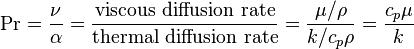
: momentum diffusivity (kinematic viscosity), \nu = \mu/\rho, (SI units: m2/s)
  • \alpha : thermal diffusivity, \alpha = k/(\rho c_p), (SI units: m2/s)
  • \mu : dynamic viscosity, (SI units: Pa s = N s/m2)
  • k : thermal conductivity, (SI units: W/m-K)
  • c_p : specific heat, (SI units: J/kg-K)
  • \rho : density, (SI units: kg/m3)


Small values of the Prandtl number, Pr << 1, means the thermal diffusivity dominates. Whereas with large values, Pr >> 1, the momentum diffusivity dominates the behavior. For example, for liquid mercury the heat conduction is more significant compared to convection, so thermal diffusivity is dominant. However, for engine oil, convection is very effective in transferring energy from an area in comparison to pure conduction, so momentum diffusivity is dominant.

In heat transfer problems, the Prandtl number controls the relative thickness of the momentum and thermal boundary layers. When Pr is small, it means that the heat diffuses quickly compared to the velocity (momentum). This means that for liquid metals the thickness of the thermal boundary layer is much bigger than the velocity boundary layer.


Reynold’s Number

As an object moves through the atmosphere, the gas molecules of the atmosphere near the object are disturbed and move around the object. Aerodynamic forces are generated between the gas and the object. The magnitude of these forces depend on the shape of the object, the speed of the object, the mass of the gas going by the object and on two other important properties of the gas; the viscosity, or stickiness, of the gas and the compressibility, or springiness, of the gas. To properly model these effects, aerodynamicists use similarity parameters which are ratios of these effects to other forces present in the problem. If two experiments have the same values for the similarity parameters, then the relative importance of the forces are being correctly modelled.

Aerodynamic forces depend in a complex way on the viscosity of the gas. As an object moves through a gas, the gas molecules stick to the surface. This creates a layer of air near the surface, called a boundary layer, which, in effect, changes the shape of the object. The flow of gas reacts to the edge of the boundary layer as if it was the physical surface of the object. To make things more confusing, the boundary layer may separate from the body and create an effective shape much different from the physical shape. And to make it even more confusing, the flow conditions in and near the boundary layer are often unsteady (changing in time). The boundary layer is very important in determining the drag of an object. To determine and predict these conditions, aerodynamicists rely on wind tunnel testing and very sophisticated computer analysis.

The important similarity parameter for viscosity is the Reynolds number. The Reynolds number expresses the ratio of inertial (resistant to change or motion) forces to viscous (heavy and gluey) forces. From a detailed analysis of the momentum conservation equation, the inertial forces are characterized by the product of the density rho times the velocity V times the gradient of the velocity dV/dx. The viscous forces are characterized by the dynamic viscosity coefficient mu times the second gradient of the velocity d^2V/dx^2. The Reynolds number Re then becomes:

Re = (rho * V * dV/dx) / (mu * d^2V/dx^2)

The gradient of the velocity is proportional to the velocity divided by a length scale L. Similarly, the second derivative of the velocity is proportional to the velocity divided by the square of the length scale. Then:

Re = (rho * V * V/L) / (mu * V / L^2)

Re = (rho * V * L) / mu

The Reynolds number is a dimensionless number.

The Reynolds number can be further simplified if we use the kinematic viscosity nu that is equal to the dynamic viscosity divided by the density:

nu = mu / rho

Re = V * L / nu

Reynolds Number is used to determine whether a flow will be laminar or turbulent. If Re is high (>2100), inertial forces dominate viscous forces and the flow is turbulent; if Re is low (<1100), viscous forces dominate and the flow is laminar.